Nature Photonics ( IF 32.3 ) Pub Date : 2025-06-03 , DOI: 10.1038/s41566-025-01694-1
S. L. Moore, H. Y. Lee, N. Rivera, Y. Karube, M. Ziffer, E. S. Yanev, T. P. Darlington, A. J. Sternbach, M. A. Holbrook, J. Pack, X. Xu, C. R. Dean, J. S. Owen, P. J. Schuck, M. Delor, X. Y. Zhu, J. Hone, D. N. Basov
|
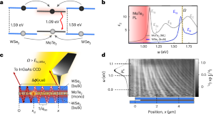
Atomically layered van der Waals (vdW) materials exhibit remarkable properties, including highly confined infrared waveguide modes and the capacity for infrared emission in the monolayer limit. Here we engineered structures that leverage both of these nano-optical functionalities. Specifically, we encased a photoluminescing atomic sheet of MoTe2 within two bulk crystals of WSe2, forming a vdW waveguide for the embedded light-emitting monolayer. The modified electromagnetic environment offered by the WSe2 waveguide alters MoTe2 spontaneous emission—a phenomenon we directly image with our interferometric nano-photoluminescence technique. We captured spatially oscillating nanoscale patterns prompted by spontaneous emission from MoTe2 into waveguide modes of WSe2 slabs. We quantify the resulting Purcell-enhanced emission rate within the framework of a waveguide quantum electrodynamics model, relating the MoTe2 spontaneous emission rate to the measured waveguide dispersion. Our work marks a substantial advance in the implementation of all-vdW quantum electrodynamics waveguides.
中文翻译:
红外纳米光致发光探测的范德华波导量子电动力学
原子层状范德华 (vdW) 材料表现出卓越的性能,包括高度受限的红外波导模式和单层极限的红外发射能力。在这里,我们设计了利用这两种纳米光学功能的结构。具体来说,我们将 MoTe2 的光致发光原子片包裹在 WSe2 的两个块状晶体中,形成嵌入式发光单层的 vdW 波导。WSe2 波导提供的改进电磁环境改变了 MoTe2 自发发射,我们用干涉纳米光致发光技术直接对这种现象进行了成像。我们捕获了由 MoTe2 到 WSe2 板的波导模式引起的空间振荡纳米级图案。我们在波导量子电动力学模型的框架内量化了得到的 Purcell 增强发射率,将 MoTe2 自发发射率与测得的波导色散相关联。我们的工作标志着全 vdW 量子电动力学波导的实现取得了重大进展。


 京公网安备 11010802027423号